
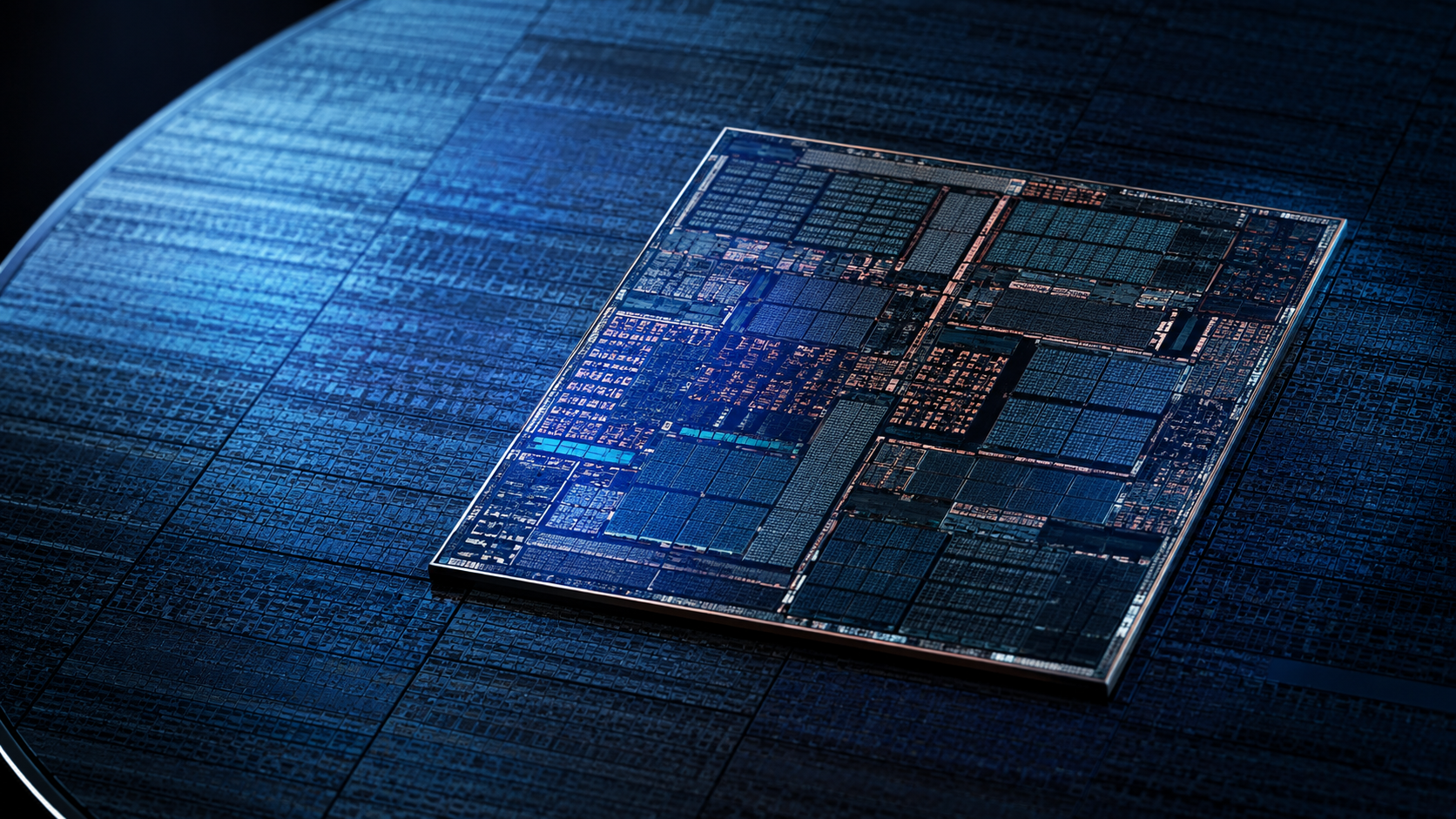
- A reported order for an Exynos 2700 version of the Galaxy S27 Ultra motherboard is a meaningful vote of confidence from Samsung’s mobile division. It is not yet proof that Exynos will replace Qualcomm across the Ultra line: the reported plan remains dual-track and region-dependent.
- The leaked die annotation points to a radically cache-heavy design: a reported 24MB system-level cache and four 4MB L3 slices, or 40MB before private CPU and GPU caches. That architecture can reduce memory traffic, latency and power, but every capacity and floorplan label remains unverified.
- SF2P probably represents a material step forward. Samsung says second-generation 2nm mobile products are ramping, and a Foundry executive has cited 15% higher frequency and 26% lower power from SF2 to SF2P. Yet more than half of those gains reportedly come from design-technology co-optimization. Retail-device thermals, yield, bin distribution and high-volume shipment—not a leaked die or internal benchmark—will be the real proof.
Introduction: Samsung Has Moved the Exynos Question to the Ultra Tier
For years, the simplest way to judge Samsung’s confidence in Exynos was to look at the Galaxy Ultra. The standard and Plus models could carry Samsung silicon in selected regions, but the Ultra—the most expensive phone, the hardest thermal envelope and the model that sets the brand’s reputation—stayed with Qualcomm. That made Snapdragon more than a component. It was insurance.
The reported Galaxy S27 plan changes that signal. MoneyToday says Samsung recently ordered a Galaxy S27 Ultra motherboard built around the Exynos 2700, after development of the Snapdragon version was already well advanced. The report describes a two-track program: Exynos for Korea and some other markets, Snapdragon retained for the United States and possibly elsewhere. If that configuration reaches stores, it would be the first Exynos return to Samsung’s top flagship tier since the Galaxy S22 generation.
That is important, but it is easy to overread. A motherboard order proves that a product branch exists. It does not prove that Samsung has approved mass production, that the branch will survive final validation, or that Qualcomm will disappear from the Ultra. The best interpretation is narrower: Samsung MX is willing to spend engineering time and supply-chain capital to qualify Exynos 2700 for its most demanding phone. That is a stronger signal than a benchmark leak, but weaker than a retail launch.
Main Analysis: Evidence of Progress, Not Yet Proof
Does the S27 Ultra report prove that Samsung Foundry’s second-generation 2nm process, SF2P, has improved dramatically? It is evidence that the full platform has improved enough to deserve qualification. It is not proof that the process itself has improved by the same amount.
A mobile SoC is a system of systems. The transistor process matters, but so do CPU intellectual property, GPU architecture, physical design, cache hierarchy, memory controller, voltage-frequency tuning, packaging, thermal spreading, modem behavior, firmware and the phone chassis. Exynos 2700 appears to change several of those variables at once. A better result cannot automatically be assigned to SF2P.
There is also a measurement problem. Foundry performance claims usually compare a test circuit at the same power, or the same speed, under specified design rules. They are not promises that a finished smartphone will be 15% faster and 26% more efficient. Samsung’s actual product may trade some process gain for more transistors, larger caches, higher clocks or a wider GPU. That is often the right engineering choice, but it means node-level percentages and handset-level battery life are different facts.
The Leak’s Most Important Detail Is 40MB of Cache
The most interesting part of the annotated die image supplied with this article is not the 4.24GHz label or the Xclipse 970 name. It is the amount of silicon apparently reserved for memory close to the compute engines.
The annotation identifies a 24MB system-level cache (SLC) and four 4MB L3 cache blocks on the CPU side. If those labels are correct, that is 40MB of shared and last-level cache before counting each CPU core’s private L2, any GPU L2, NPU local SRAM and smaller buffers. The chip’s true on-die SRAM would therefore be higher.
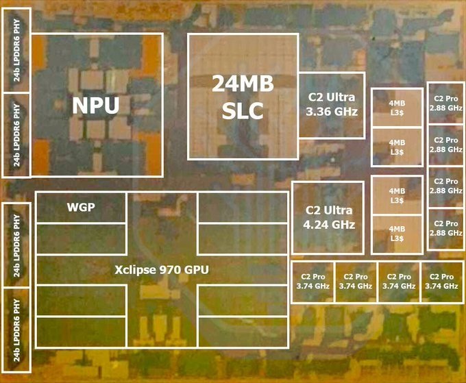
That allocation is a strategic choice. Smartphone SoCs have a fixed area budget shared by the CPU, GPU, NPU, image processor, memory interfaces, security blocks and interconnect. A cache block does not create benchmark headlines by itself, yet it occupies valuable silicon. If the drawing is broadly accurate, Samsung chose to spend a surprisingly large part of its 2nm density dividend on data movement.
That can be rational because moving data is expensive. Accessing a nearby cache is much faster and usually consumes far less energy than going off-chip to LPDDR memory. A large SLC can absorb traffic from CPU, GPU, NPU and imaging workloads; reduce pressure on the memory controller; and keep execution units busy. It can be particularly valuable in gaming, on-device AI and computational photography, where several engines compete for bandwidth.
The approximate 8% area estimate should be treated carefully. The image is low resolution, boundaries may be stylized, and density differs by macro. SRAM also scales differently from logic. Still, the basic conclusion survives: Samsung appears to be trading die area for a wider energy-efficient memory hierarchy.
Why a Cache-Heavy Design Could Fix the Exynos 2600’s Weak Spot
The design makes more sense when placed against the Exynos 2600. Samsung’s official material presents the 2600 as the first 2nm GAA mobile processor, with a ten-core Arm CPU, Xclipse 960 graphics, a much stronger NPU and a Heat Path Block package designed to reduce thermal resistance. Independent analysis was more mixed.
Geekerwan’s analysis, summarized by Notebookcheck, estimated that the Xclipse 960 GPU occupied about 23% of the Exynos 2600 die and delivered roughly 7 teraflops of theoretical compute, yet carried only 2MB of GPU L2 cache. Under bandwidth-heavy work, the GPU could run into an external-memory wall. Android Authority’s sustained gaming tests also found that performance could fall sharply after roughly ten minutes in demanding titles as the phone warmed.
That does not mean the 2600 was a failure. It means peak compute had outrun the system’s ability to feed and cool it. Exynos 2700’s reported remedy is architectural, not cosmetic: more shared cache, possible growth in GPU uncore and cache, LPDDR6 physical interfaces, and a CPU layout mixing lower-clock C1 cores with newer high-performance C2 cores.
The leaked ten-core layout is unusual. The annotation shows one C1-Ultra at 3.36GHz with four C1-Pro cores at 2.88GHz, plus one C2-Ultra at 4.24GHz and four C2-Pro cores at 3.74GHz. Notebookcheck argues that the older C1 group could handle sustained efficient work while the C2 group supplies short bursts. That would give Samsung more points on the power-performance curve than the 2600’s one-prime-plus-nine-middle arrangement. But the labels are derived from an engineering sample and can still change.
What SF2P Officially—or Semi-Officially—Promises
The strongest process evidence does not come from the die leak. It comes from Samsung’s roadmap and corporate disclosures.
Samsung Electronics said in its second-quarter 2026 results that Foundry planned to ramp new mobile products based on its second-generation 2nm process in the second half. System LSI also reported strong mobile SoC momentum. Samsung did not name Exynos 2700, but the timing and product class line up.
Separately, TrendForce quoted a report based on comments from Shin Jong-shin, vice president of Samsung Foundry’s Design Platform Development Team. Moving from SF2 to SF2P was said to cut power by 26% and raise operating frequency by 15%. The crucial detail was that more than half of the gain reportedly came from design-technology co-optimization, or DTCO.
DTCO means the process and the chip design are tuned together: standard-cell libraries, wiring, SRAM macros, power delivery and physical-design rules are altered so real products extract more value from the transistors. That is good news, not a qualification. A foundry customer buys usable design outcomes, not transistor physics in isolation. But it does mean the headline numbers cannot be described as pure transistor improvement.
Earlier reports cited slightly different figures—about 12% more performance, 25% less power and 8% less area. Those numbers may reflect earlier targets, different test vehicles, different comparison points or rounding. Until Samsung releases a formal SF2P design-rule comparison, the safest range is to say that industry reports point to a mid-teens frequency gain and roughly one-quarter lower power under controlled conditions.
Internal Benchmarks Are Encouraging—and Incomplete
Yonhap reported that Samsung MX compared Exynos 2700 with Qualcomm’s next Snapdragon 8 Elite generation in internal tests. In Geekbench 6.5 multi-core, Exynos reportedly led the standard Snapdragon by 19% and the higher-end Pro version by 9.5%. Peak GPU performance was said to be 5% ahead of the Pro chip; at a 2.5-watt GPU operating point, the lead was reported at 22%–24%. A Llama 3.1 8B test showed an 18% advantage in response generation, while a simulated usage test measured 161mA for Exynos versus 185mA for Snapdragon Pro, a 12.7% reduction.
Those are exactly the results Samsung would need to justify an Ultra design. The low-power GPU number is more informative than a peak score because smartphones live inside strict thermal limits. The 161mA system result is also potentially important, though the workload, display, modem state, memory configuration and software build must be identical for a clean comparison.
Still, these are internal figures reported through industry sources. Neither final chip was a retail product, and Qualcomm has not validated the comparison. A public Geekbench AI entry associated with the S5E9975 identifier supports the existence of a ten-core engineering sample running up to 4.24GHz, but it does not establish CPU or sustained-device performance. Internal benchmarks move the probability. They do not close the case.
Ultra Qualification Is a Stronger Signal Than a Benchmark
Why take the motherboard order seriously at all? Because Samsung MX has different incentives from Samsung System LSI and Foundry. System LSI wants its chip adopted; Foundry wants wafer volume. MX owns the consumer experience, warranty risk and the commercial damage if two regional versions behave differently. It can choose Qualcomm even when that is more expensive.
An Ultra qualification therefore implies that the reported Exynos sample has cleared—or is close enough to clearing—internal thresholds for performance, thermal behavior, camera pipelines, modem compatibility and supply. Adding the Exynos branch after Snapdragon development was well advanced is costly. Companies do not usually do that merely to flatter an internal supplier.
But qualification also serves bargaining and resilience. Maintaining two viable platforms reduces dependence on Qualcomm, improves negotiating leverage and provides a hedge against allocation or pricing shocks. Samsung reportedly spent 7.44 trillion won on externally sourced mobile application processors in the first half of 2026, equal to 17.9% of DX division raw-material costs. Even partial substitution can matter. Dual sourcing can be economically rational before Exynos is technically dominant.
Why the Die Itself Does Not Prove Yield
A successful engineering sample proves that at least one working die exists. Yield is the percentage of good dies across many wafers, at the voltage and clock bins required for sale. Those are different things.
The cache-heavy design may even make yield more demanding. Larger dies expose more area to random defects. SRAM arrays are dense and repetitive, which enables redundancy and repair, but they also impose tight stability requirements at low voltage. A 40MB shared-cache design can be excellent for energy efficiency while simultaneously increasing die cost if defect density remains high.
Samsung can manage that trade-off through better defect density, redundancy, binning and volume learning. If Exynos 2700 ships across a large share of Galaxy S27 units—including Ultra models—that would indirectly imply that yield and cost are acceptable. It still would not reveal a precise yield percentage. The often-repeated “95% process capability” wording in Korean reports should not be automatically converted into a 95% wafer yield; it is an ambiguous engineering claim, not a disclosed yield table.
A Practical Proof Ladder for SF2P
| Evidence | What it tells us | What it does not prove |
|---|---|---|
| Samsung’s official second-generation 2nm mobile ramp | The process and at least one mobile product have entered a manufacturing phase | Exynos 2700 specifications, yield or Galaxy model allocation |
| Reported S27 Ultra motherboard order | MX is funding and validating an Exynos Ultra branch | Final launch, global Qualcomm replacement or sales volume |
| Internal performance and power comparisons | The current sample may meet Samsung’s decision thresholds | Independent, sustained retail performance |
| Public engineering-sample database entry | A ten-core S5E9975-class chip running up to 4.24GHz likely exists | Final clocks, thermal behavior or battery life |
| Leaked 24MB SLC and 16MB L3 annotation | Samsung may be pursuing a cache-heavy architecture | Authenticity, exact capacity, physical area or production design |
| High-volume retail shipment in several markets | Yield, cost and platform quality are commercially acceptable | Exact defect density or foundry competitiveness for external customers |
| Independent same-chassis comparison | Real battery, heat, camera, gaming and modem differences | Foundry process gains separated from design and software |
| Major external SF2P customers | The process is competitive beyond Samsung’s captive ecosystem | That every product on the node will perform equally well |
Investment Implications: More Than Saving a Qualcomm Bill
For Samsung Electronics, a successful Exynos 2700 would create value in three places. MX could reduce external component spending and improve procurement leverage. System LSI could spread design costs over more units. Foundry could fill advanced-node capacity and learn faster from high-volume production. Those benefits reinforce one another.
The strategic value may be larger than the phone’s direct margin. Advanced foundry customers care about demonstrated volume, libraries, packaging and delivery discipline. A strong Exynos launch would give Samsung a reference product for SF2P and improve the credibility of its broader 2nm roadmap. Conversely, a throttling controversy in the Ultra line would damage both the mobile brand and foundry narrative at once.
Qualcomm would not vanish. The reported plan retains Snapdragon in the United States, where modem certification and operator relationships matter, and possibly in other high-value markets. Qualcomm also sets the external performance benchmark and can price aggressively to defend share. The more likely outcome is a better-balanced dual-source relationship, not an overnight divorce.
What Investors and Buyers Should Watch
- Model allocation: Is Exynos limited to the standard S27, or does an Ultra version actually ship? In which countries?
- Volume: Does Exynos approach the roughly 50% S27-family share discussed by Korean analysts, or remain a small qualification run?
- Sustained performance: Compare 20- and 30-minute gaming, camera recording and AI workloads—not one-minute peaks.
- Energy at equal work: Battery drain at the same frame rate or inference throughput matters more than maximum benchmark scores.
- Modem behavior: Standby drain, weak-signal power and carrier aggregation can erase an efficient application processor’s gains.
- Die size and package: A large cache is valuable only if Samsung can manufacture and cool it at an acceptable cost.
- External customer wins: A credible non-Samsung SF2P design would be the clearest sign that foundry competitiveness is broadening.
Conclusion: The Turning Point Will Be Measured in Stores, Not Leaks
Exynos 2700 is shaping up as Samsung’s most consequential mobile chip in years. The reported S27 Ultra motherboard order says MX sees enough potential to qualify its in-house silicon for the company’s most unforgiving product. The leaked floorplan says Samsung may be attacking the right problem: not merely adding compute, but spending substantial die area on a cache hierarchy that reduces data movement and improves sustained efficiency. Reported internal tests point in the same direction.
Together, those signals make a persuasive case that SF2P and the surrounding design platform have advanced. They do not isolate the process contribution, establish mass-production yield or guarantee retail performance. The design may owe as much to DTCO, Arm’s new cores, AMD-derived graphics, a larger cache and improved packaging as to transistor-level gains.
The decisive evidence will arrive in a sequence: final Ultra allocation, meaningful shipment volume, same-chassis independent testing, and eventually external SF2P customer wins. If Samsung clears all four gates, Exynos 2700 will be more than a good phone chip. It will mark the moment Samsung’s 2nm foundry platform becomes commercially credible again.
Related Topics
- How system-level cache changes mobile GPU and on-device AI economics
- Samsung SF2P versus TSMC N2P: why node labels are insufficient
- Dual sourcing as procurement leverage in premium smartphones
- The role of advanced packaging and heat spreading in mobile SoCs
- Why foundry yield cannot be inferred from a single benchmark sample
Sources and Further Reading
- MoneyToday, “Samsung’s Exynos to Return to Galaxy Ultra Flagship After Five Years,” Sept. 1, 2026.
- Samsung Electronics, Q2 2026 results and second-generation 2nm mobile ramp.
- TrendForce, SF2P roadmap and DTCO contribution, July 2, 2026.
- The Elec, Samsung Foundry 2nm platform roadmap.
- Yonhap News, Exynos 2700 internal benchmark report, Aug. 23, 2026.
- Yonhap News, Exynos 2700 production-sample timeline and S27 share outlook, Mar. 4, 2026.
- The Korea Herald, “Samsung pushes Exynos 2700 to cut Qualcomm reliance,” Mar. 2026.
- Seoul Economic Daily, Exynos 2700 internal comparison and AP spending.
- Herald Business, Exynos 2700 performance and efficiency claims.
- Notebookcheck, annotated die analysis, Sept. 3, 2026.
- SemiAnalysis, reported Exynos 2700 die image.
- Piglin, CPU block-label corrections to the die annotation.
- Notebookcheck, S5E9975 Geekbench AI sample analysis, Aug. 23, 2026.
- Geekbench Browser, public AI benchmark record associated with S5E9975.
- Geekerwan, Exynos 2600 die, GPU and sustained-performance analysis.
- Samsung Semiconductor, official Exynos 2600 product specifications.
- Samsung Newsroom, GAA/MBCFET and DTCO background.
- Samsung Semiconductor, 2nm foundry roadmap at SFF 2024.
- Samsung and AMD, multi-generation Radeon IP agreement for Exynos.
- Android Authority, sustained Exynos 2600 gaming comparison.
- Android Authority, Exynos 2600 heat and throttling tests.
- Android Authority, technical requirements for Exynos 2700.
- GSMArena, S27 Ultra dual-platform report, Sept. 2, 2026.
- GSMArena, early Exynos 2700 specifications leak and source caveat.
- Digital Trends, interpretation of reported Exynos 2700 tests and limitations.
- SamMobile, reported CPU, GPU, AI and power comparisons.
Language versions:
한국어 원문 |
English version