
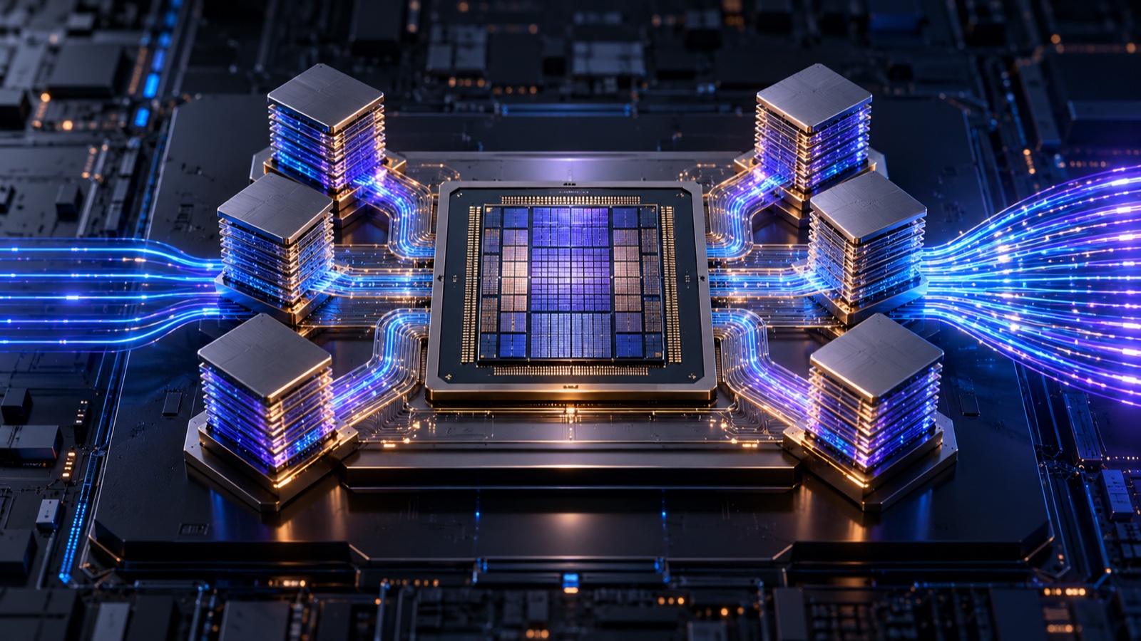
HBM4 is a structural break in accelerator memory design, not merely a faster generation of DRAM. The standard doubles the interface per stack from 1,024 bits in HBM3 and HBM3E to 2,048 bits. That width increase is the largest single contributor to the jump from NVIDIA B200’s up-to-8 TB/s memory bandwidth to Rubin’s up-to-22 TB/s. The next step is less straightforward. Public HBM4E designs retain 2,048 I/O and target as much as 16 Gb/s per pin, implying roughly 4 TB/s per stack. There is no finalized JEDEC HBM5 specification, and NVIDIA has not disclosed official memory-bandwidth figures for Rubin Ultra or Feynman.
Executive summary
- The hypothesis is partly supported. HBM4’s 2x interface-width increase is a one-time structural lever within the published roadmap and helps explain the roughly 2.75x B200-to-Rubin bandwidth increase.
- HBM4E is unlikely to repeat that per-GPU jump through pin speed alone. At 2,048 bits and 16 Gb/s, theoretical bandwidth is 4.096 TB/s per stack—about 1.49x Rubin’s implied 2.75 TB/s per stack, assuming eight stacks.
- This is not the end of AI performance scaling. It raises the value of cache, locality, quantization, KV-cache compression, speculative decoding, MoE, NVLink, rack-scale fabrics and alternative memory architectures, especially for decode-heavy inference.
From HBM2 to HBM4E: the verified bandwidth curve
A useful first-order identity is bandwidth ≈ interface width × per-pin data rate × number of HBM stacks. Per-stack figures below are theoretical or vendor-rated; realized accelerator bandwidth also reflects controller efficiency, channel configuration and product binning.
| Generation | Interface per stack | Representative pin rate | Bandwidth per stack | Typical capacity / height | Introduction | Representative NVIDIA accelerator / stacks / aggregate bandwidth |
|---|---|---|---|---|---|---|
| HBM2 | 1,024-bit | 1.6–2.4 Gb/s | 205–307 GB/s | 4–8 GB, 4H/8H | 2016–2017 | V100 / 4 / up to 900 GB/s |
| HBM2E | 1,024-bit | 3.2–3.6 Gb/s | 410–461 GB/s | 8–16 GB, mainly 8H | 2019–2021 | A100 80GB / 5 active stacks / 2.039 TB/s |
| HBM3 | 1,024-bit | Up to 6.4 Gb/s | Up to 819 GB/s | 16–24 GB, 8H/12H | 2021–2022 | H100 SXM / 5 / 3.35 TB/s |
| HBM3E | 1,024-bit | About 8–9.6 Gb/s | About 1.0–1.23 TB/s | 24–36 GB, 8H/12H | 2024 | H200 / 6 placements / 4.8 TB/s; B200 / 8 placements / up to 8 TB/s |
| HBM4 | 2,048-bit | JEDEC 8 Gb/s; vendors 10–13 Gb/s | 2.048–3.328 TB/s | 24–48 GB, 8H/12H/16H | 2025 standard; 2026 ramp | Rubin / 8S on NVIDIA roadmap / up to 22 TB/s |
| HBM4E | 2,048 I/O retained | Up to 16 Gb/s | Up to 4.096 TB/s theoretical | 32–64 GB, 8H/12H/16H planned | 2026 samples; 2027 volume target | Rubin Ultra / 16S on roadmap / official GPU bandwidth not disclosed |
| HBM5 | Not specified | Not specified | Not specified | Not specified | No finalized JEDEC standard | Feynman says “Next-Gen HBM”; no official bandwidth |
NVIDIA’s official specifications confirm 3.35 TB/s for H100 SXM, 4.8 TB/s for H200 and up to 8 TB/s for B200. Rubin is specified with 288 GB of HBM4 and up to 22 TB/s. The company has not published an official Rubin Ultra bandwidth number, nor a Feynman memory-bandwidth specification. Claims such as “F200 at 30+ TB/s” should therefore not be treated as product specifications.
Why HBM4 is different: the 2x interface
HBM3 and HBM3E use approximately 1,024 data I/O per stack. JEDEC’s HBM4 standard doubles that to 2,048. Samsung and SK hynix explicitly describe the transition as a move from 1,024 to 2,048 I/O. At an unchanged pin rate, this alone doubles theoretical per-stack bandwidth.
Using the rounded accelerator specifications and an eight-stack package for both B200 and Rubin illustrates the source of the 2.75x increase:
| Driver | B200 / HBM3E | Rubin / HBM4 | Approximate contribution |
|---|---|---|---|
| Interface width per stack | 1,024-bit | 2,048-bit | 2.00x |
| Implied pin rate from aggregate bandwidth | ~7.81 Gb/s | ~10.74 Gb/s | ~1.38x |
| HBM stack count | 8 placements | 8S | 1.00x |
| Combined effect | Up to 8 TB/s | Up to 22 TB/s | ~2.75x |
The result matters strategically. HBM4 is not just a faster DRAM die. Doubling I/O changes the GPU-side PHY and memory-controller footprint, micro-bump count, silicon-interposer routing density and logic-base-die complexity. It shifts more value toward advanced packaging and co-design among GPU vendors, memory suppliers and foundries.
What changes with HBM4E
Public Samsung and SK hynix HBM4E disclosures retain the 2,048-I/O interface and raise the data rate to as much as 16 Gb/s. The arithmetic is straightforward:
2,048 bits × 16 Gb/s ÷ 8 = 4.096 TB/s per stack.
Rubin’s 22 TB/s over eight stacks implies approximately 2.75 TB/s per stack, or about 10.74 Gb/s per pin. Moving to 16 Gb/s while keeping eight stacks would produce a theoretical 32.8 TB/s, roughly 1.49x Rubin—not another 2.75x leap.
NVIDIA’s 2025 roadmap labels Rubin Ultra as “16S HBM4E.” Doubling the number of stacks could lift aggregate bandwidth much more sharply, but that would be a package- and system-level scaling choice rather than another doubling of interface width per stack. It also carries costs in interposer area, power delivery, cooling, yield and memory capacity. Until NVIDIA publishes a product specification, raw sums based on 16 stacks should be treated as scenario math, not official Rubin Ultra bandwidth.
A necessary distinction: 12-high and 16-high increase capacity, not peak bandwidth
Moving from an 8-high HBM stack to 12-high or 16-high primarily increases capacity. Peak bandwidth per stack is set by the external interface width and per-pin data rate. Adding DRAM dies does not multiply the external channels: the dies share the stack’s I/O. More banks and scheduling opportunities may improve realized bandwidth in some workloads, but stack height alone does not raise nameplate bandwidth in proportion to layer count.
The post-HBM4 question is therefore not simply how high HBM can be stacked. It is which of four bandwidth levers can scale economically.
| Lever | Bandwidth effect | Principal constraint | Prospect around HBM5 |
|---|---|---|---|
| Higher pin rate: 16→20 Gb/s+ | Linear per stack | Energy per bit, signal integrity, heat | Incremental gains are plausible, but increasingly power-expensive |
| More stacks per package: 8→12→16 | Linear at GPU or system level | Interposer area, CoWoS-class capacity, yield, cost and cooling | Rubin Ultra’s 16S roadmap points this way; official bandwidth is undisclosed |
| Wider interface: 2,048→4,096 | 2x per stack at the same pin rate | Host PHY area and shoreline, bump/TSV count, routing and base-die design | A KAIST research-roadmap scenario, not a finalized JEDEC direction |
| Direct 3D integration such as HBM-on-logic | Potentially very high internal bandwidth | Thermals, yield, power delivery and co-design | A longer-term post-HBM5 direction; no shipping standard or firm schedule |
Could width scaling return with HBM5?
At the physics level, a wider and slower link is generally more energy-efficient than a narrower link driven at a much higher speed. As data-center constraints shift toward power delivery and cooling, pushing pins beyond 20 Gb/s becomes an expensive way to add bandwidth. HBM adopted a wide, relatively slow interface rather than a GDDR-like high-speed bus for precisely this reason. On that basis, renewed width scaling in HBM5 is a credible engineering scenario.
The harder constraint is the host accelerator’s PHY area and die-edge “shoreline.” HBM4 introduces advanced-logic base dies that can be customized for a customer. Industry design work is exploring moving memory-controller functions into that base die and connecting it to the accelerator through UCIe or another die-to-die interface. This can decouple the very wide internal TSV interface from the host-side PHY, reducing pad and driver area on the expensive compute die. It is a potentially important path to wider memory, but it is a custom-HBM architecture concept—not confirmation that HBM5 will standardize 4,096 bits or UCIe.
Hybrid bonding has a similar distinction. It does not create external bandwidth on its own. Its bump-less fine pitch can accommodate denser TSV/I/O connections and taller stacks while reducing interconnect length and thermal resistance, making wider interfaces easier to build. Yet JEDEC’s relaxation of nominal HBM4 package thickness to 775µm for both 12-high and 16-high stacks gives TC bonding more runway. Industry research now places broader hybrid-bonding adoption around 16-high HBM4E or 20-high HBM5, with timing likely to vary by supplier.
KAIST TERA Lab’s long-term academic roadmap assumes 4,096 I/O at roughly 8 Gb/s for HBM5—about 4 TB/s per stack—then 4,096 I/O at 16 Gb/s for HBM6 and 8,192 I/O for HBM7. This is useful evidence that renewed width scaling is a serious research scenario. It is not a JEDEC specification, a memory-vendor product commitment or an NVIDIA roadmap. The evidence therefore does not support either extreme claim: HBM4 is not proven to be the last width doubling ever, but 4,096-bit HBM5 cannot yet be treated as the base case.
Two investable paths
If width expansion materializes, more value should accrue to logic-base-die foundries, custom-HBM IP and design services, hybrid-bonding tools, and large-interposer/CoWoS-class capacity. TSMC can potentially manufacture both an external customer’s accelerator and base die, while Samsung retains option value from vertical integration across memory, foundry and packaging. The long-term counterpoint is substitution risk for equipment tied mainly to micro-bump TC bonding.
If width expansion is delayed, more stacks, larger interposers, higher pin rates and stronger cooling become the practical means of defending aggregate bandwidth. Packaging, substrates, power delivery and liquid cooling then carry more leverage. Advanced packaging is the common beneficiary in both scenarios, making package area, yield and energy per bit more useful investment indicators than a single forecast for HBM5 interface width.
HBM5: separate standards from roadmaps
As of October 2026, the public evidence falls into distinct categories:
- JEDEC-confirmed: JESD270-4 defines HBM4 with a 2,048-bit interface. A finalized HBM5 specification has not been published.
- Vendor roadmaps: Samsung has shown an HBM5 direction at FMS 2026, while SK hynix discusses hybrid bonding and cooling for future HBM generations. These are not interface-width or bandwidth standards.
- NVIDIA roadmap: Feynman is associated with “Next-Gen HBM,” but NVIDIA has not confirmed HBM5, a 4,096-bit interface or an aggregate memory-bandwidth number.
- Industry reports and analyst estimates: These may be useful scenarios, but they should not be presented as JEDEC or NVIDIA specifications.
There is therefore no official basis for assuming that HBM5 will use a 4,096-bit interface. HBM4 may prove to be the last width-doubling generation for some time, but “last ever” is not established.
Stack height is not a bandwidth lever
Moving from 12-high to 16-high primarily adds capacity; it does not directly raise peak bandwidth per stack. A stack’s theoretical bandwidth is set mainly by interface width multiplied by per-pin data rate. Additional DRAM dies share the existing channels. More banks and better scheduling may improve realized bandwidth modestly, but this is not the same structural gain as widening the interface.
| Lever | Bandwidth effect | Principal constraint | Evidence level for the HBM5 timeframe |
|---|---|---|---|
| Higher pin rate (16→20+ Gb/s) | Linear with speed | Energy per bit, signal integrity, thermals | Incremental gains fit vendor roadmaps, but efficiency worsens |
| More stacks per package (8→12→16) | Linear at GPU or system level | Interposer size, CoWoS-L-class capacity, yield, cost, cooling | NVIDIA’s Rubin Ultra 16S is an official roadmap item; aggregate bandwidth is not disclosed |
| Wider interface (2,048→4,096 I/O) | Up to 2x at the same pin rate | GPU PHY shoreline, bump pitch, TSV and routing density, co-design | A candidate in an academic roadmap and industry inference, not a confirmed JEDEC or vendor specification |
| Direct 3D memory-on-logic stacking | Potentially very large | Thermals, cumulative yield, test and co-design | A long-term research path, not an official HBM5 schedule |
4,096 I/O is a possible HBM5 scenario, not a standard
Under a power constraint, a wide, slower link generally offers better transfer-energy and signal-integrity economics than a narrow, very fast link. This is also why HBM adopted a much wider and slower interface than GDDR. A combination of 4,096 I/O and a moderate pin-rate increase is therefore a credible HBM5 scenario worth testing. As of October 2026, however, there is no finalized JEDEC HBM5 specification, and Samsung, SK hynix and Micron have not confirmed 4,096 I/O as a product specification.
A custom logic base die could be an enabling mechanism. HBM4’s move toward foundry-manufactured, customer-specific logic base dies creates room to place more controller or interface functions beneath the DRAM. In principle, designers could preserve a very wide internal DRAM connection while concentrating the GPU-facing side into a dense die-to-die link, reducing the GPU die-edge PHY burden. But an HBM5 architecture combining 4,096-bit DRAM-side connectivity with a UCIe-like GPU link is industry inference, not a disclosed JEDEC design or vendor product architecture. TSMC N12/N3-class options and Samsung’s vertically integrated foundry position belong to vendor and customer programs, not the HBM5 standard.
SK hynix’s hybrid-bonding technical note describes the benefits of finer pitch, higher connection density, lower power and lower thermal resistance. Hybrid bonding does not create bandwidth by itself, but it can enable denser I/O and taller stacks. Vendor commentary also notes that JEDEC’s increase in the HBM4 package-height envelope from 720 μm to 775 μm gives conventional bonding more room through HBM4, potentially deferring broad hybrid-bonding adoption to high-stack HBM4E or HBM5.
KAIST TERA is an academic roadmap
The KAIST TERA Lab long-term roadmap and workshop material released in 2025 model HBM5 with 4,096 I/O, roughly 8 Gb/s and approximately 4 TB/s per stack, followed by later generations that again increase data rate or width. This is a research-lab proposal—not a JEDEC standard, a memory-vendor production commitment or an NVIDIA product specification. It is nevertheless a concrete academic counterexample to the claim that HBM4 must be the final width expansion.
The evidence is clearer when divided into four layers. Official specifications confirm 2,048 I/O only through HBM4. Vendor and customer roadmaps show HBM4E speed scaling, Rubin Ultra 16S, and future bonding and base-die directions, but do not confirm 4,096-I/O HBM5. The academic roadmap is KAIST TERA’s 4,096-I/O scenario. The industry inference is that a custom base die and dense die-to-die link could decouple the DRAM-side width from the GPU-side PHY burden.
Risks and investment implications
The central risk is that 4,096 I/O may turn HBM from a broadly reusable memory product into a customer-specific co-designed component. Base-die design, validation, yield learning and customer qualification would become more expensive, and a delay at the GPU, foundry or memory supplier could postpone the entire transition. If that path slips, the industry is likely to rely longer on higher pin rates and more stacks per package.
If width expansion succeeds, value should migrate toward logic-base-die foundry capacity, custom design, hybrid-bonding equipment and fine-pitch metrology and inspection. TSMC is a candidate external base-die foundry, while Samsung’s memory-foundry integration provides strategic option value; actual share will depend on customer-specific yield and qualification. Hybrid-bonding tool vendors gain an opportunity, while suppliers concentrated in conventional thermo-compression bonding face long-run substitution risk. If width expansion is delayed, larger stack counts and package footprints increase leverage to large interposers, CoWoS-L-class capacity, substrates, power delivery and cooling. Advanced packaging benefits in both cases, although yield, capital intensity and customer concentration remain material risks.
Updated verdict: HBM4 is the latest officially confirmed doubling of interface width, but it is too early to call it the last. Retaining 2,048 I/O while raising speed and stack count is the base path through HBM4E. Beyond that, 4,096-I/O HBM5 is an upside scenario supported by an academic roadmap and a plausible design inference—not by a finalized standard. The original hypothesis remains a useful baseline, but the KAIST roadmap and custom-base-die option make it somewhat too conservative.
Why repeated width doubling is difficult
- PHY and controller area: A 2,048-bit interface consumes more die-edge and logic area. Another doubling would compete directly with compute and cache resources.
- Bump count and interposer routing: More signals require denser micro-bumps and routing layers. Crosstalk, insertion loss and power integrity become harder to control.
- Package size and yield: More stacks and wider interfaces expand the interposer and substrate, increasing assembly cost and cumulative yield risk.
- Power and thermals: More I/O and higher pin rates increase data-movement energy. Samsung specifically notes the power and thermal challenge created by HBM4’s doubled I/O.
- Signal integrity: Raising speed while increasing channel count reduces timing and voltage margins, making validation substantially more complex.
- Logic-base-die complexity: HBM4 brings more customer-specific logic into the base die, requiring tighter memory-foundry-GPU co-optimization.
Three scenarios for the bandwidth curve
| Scenario | Technology path | Bandwidth implication | What to monitor |
|---|---|---|---|
| Bull | High-density hybrid bonding, larger 2.5D/3D packages, new or serialized interfaces, more stacks | Large generational gains continue | 16 Gb/s yields, 16-stack packages, new JEDEC interface proposals |
| Base | 2,048 I/O retained; pin rate, stack count and controller efficiency improve | Incremental per-stack gains; package scale sustains system growth | 12–16 Gb/s volume ramp, advanced-packaging capacity, energy per bit |
| Bear | Thermal, power, signal-integrity and yield constraints slow pin-rate progress | Bandwidth grows materially slower than compute | Down-binning, cooling cost, package yields and qualification delays |
The base case best matches current public roadmaps: HBM4E keeps the width and raises speed. The bull case remains plausible because hybrid bonding, 3D integration or a new interface topology could create another structural step. The memory wall is a moving constraint, not a fixed ceiling.
Inference implications: prefill is not decode
It is imprecise to say that all AI inference is bandwidth-bound. LLM inference has two distinct phases. Prefill processes input tokens in parallel and is usually compute-intensive. Decode generates tokens autoregressively, repeatedly streaming model weights and reading or updating the KV cache. At low to moderate batch sizes, decode is commonly memory-bandwidth-bound. NVIDIA makes the same distinction in its Rubin and Dynamo materials, describing generation as fundamentally constrained by the memory subsystem.
The boundary moves with workload design. Larger batches reuse weights across more tokens and raise arithmetic intensity, potentially shifting the bottleneck toward compute. Long contexts enlarge the KV cache, but paged attention, cache reuse and hit rates influence actual traffic. MoE reduces active parameters per token but adds routing and inter-GPU communication. Quantization lowers bytes moved for weights and KV cache, with accuracy and kernel-efficiency trade-offs. Tensor Core utilization, network topology and collective communication can dominate at rack scale.
How architectures can respond
Even if raw HBM bandwidth grows more slowly, useful tokens per second can improve through several layers:
- larger on-chip caches and better weight/KV locality;
- FP8, FP4 and low-precision KV caches that reduce bytes transferred;
- speculative decoding and continuous batching;
- MoE models that activate fewer parameters per token;
- NVLink and rack-scale fabrics that coordinate memory and compute across GPUs;
- custom accelerators and SRAM-heavy inference architectures; and
- new memory tiers, 3D integration and potentially different HBM interfaces.
Semiconductor investment implications
First, HBM4 expands the investment opportunity beyond DRAM wafers. A 2,048-I/O interface, logic base dies, hybrid bonding, silicon interposers, advanced substrates, testing and liquid cooling all become more important. Competitive differentiation among Samsung, SK hynix and Micron will depend not only on pin rate but also on customer co-design, base-die foundry execution and package yield.
Second, slower per-stack scaling raises the value of stack count and packaging area. More HBM placements can defend aggregate bandwidth, but they consume scarce advanced-packaging capacity and increase power, cooling and yield risk. This supports demand across the advanced-packaging supply chain while also making package economics a potential limiter on accelerator shipments.
Third, investors should look beyond headline TB/s. Bytes moved per generated token, capacity, energy per bit, software optimization and rack utilization determine inference economics. If bandwidth becomes more constraining, NVIDIA’s system and software assets—NVLink, Dynamo and TensorRT-LLM—may become more defensible. The same constraint also creates room for custom ASICs, SRAM-rich accelerators and models designed around memory efficiency.
Conclusion
HBM4 is the latest officially confirmed doubling of interface width, but it is too early to conclude that it will be the last major width-driven leap. The move to 2,048 bits is the central structural reason Rubin can reach up to 22 TB/s versus B200’s up-to-8 TB/s. HBM4E keeps that width and relies on higher pin rates, so per-stack growth is likely to become more incremental. Yet there is no finalized HBM5 specification, and package scale, new interfaces, cache, software and rack-level architecture can still produce major system gains. The defensible conclusion is not that AI GPU performance will stop improving, but that memory-bandwidth scaling could become a more important constraint on future inference performance and economics.
Sources
- NVIDIA, HGX H100/H200/B200 Components
- NVIDIA, HGX Platform and Rubin specifications
- NVIDIA, Inside Rubin GPU Architecture
- NVIDIA, Inside the Rubin Platform
- NVIDIA, GTC 2025 roadmap highlights
- NVIDIA, Tesla V100
- NVIDIA, HGX A100 80GB
- NVIDIA, Hopper Architecture In-Depth
- NVIDIA, Dynamo and inference phases
- NVIDIA, NVFP4 KV Cache
- JEDEC, JESD270-4 HBM4 standard
- Samsung Electronics, HBM product portfolio
- Samsung Electronics, HBM4E at GTC 2026
- Samsung Electronics, commercial HBM4 shipment
- SK hynix, HBM2 and HBM2E specifications
- SK hynix, HBM4 and HBM4E specifications
- SK hynix, hybrid bonding and future HBM
- Micron, HBM4 product page
- Samsung Electronics, FMS 2026 HBM5 roadmap
- KAIST TERA Lab, HBM milestone and long-term roadmap
- Semiconductor Engineering, custom HBM base-die and die-to-die interfaces
- TrendForce, HBM4 package height and hybrid-bonding timing
- TrendForce, hybrid bonding for high-stack-count future HBM
This article is an industry analysis based on public technical specifications and roadmaps, not a recommendation to buy or sell any security.