
Revised: July 21, 2026 | Category: Technology
Summary
- HBM is a memory architecture that places DRAM stacks beside a GPU or AI ASIC and uses TSVs and a silicon interposer to create ultra-wide-bandwidth connections; from HBM1 through HBM3E, it has steadily improved bandwidth, capacity, and power efficiency, reducing key bottlenecks in AI training and inference.
- The biggest change in HBM4 is that it expands the HBM3E-class 1,024-bit interface to 2,048 bits and, under the JEDEC standard, introduces 32 independent channels, two pseudo-channels per channel, 12-high and 16-high stacks, improved base dies, and voltage options that define standard bandwidth of up to roughly 2TB/s per stack.
- HBM4 is expected to be used in officially discussed next-generation AI server platforms such as NVIDIA Vera Rubin and AMD Helios and MI400-class systems, while HBM4E and custom HBM are likely to spread into follow-on platform families around 2027 with customer-specific base dies and higher pin speeds, although specific models remain uncertain.
(Advertisement)
Why HBM4 Matters
The reason HBM4 matters is not simply that memory is moving forward by one generation. Since 2023, investment in AI servers has evolved into a complex industry in which the number of GPUs, network bandwidth, power delivery capacity, cooling infrastructure, advanced packaging capacity, and HBM supply all interact. In particular, for large language models, multimodal models, long-context inference, agentic AI, and Mixture-of-Experts training and inference, overall system performance is limited if the required parameters, KV cache, activations, and intermediate tensors cannot be read and written quickly enough, no matter how fast the compute engines are. In the end, the real-world performance of an AI accelerator is determined not only by FLOPS, but also by memory capacity, memory bandwidth, memory power efficiency, and the quality of the connections inside the package.
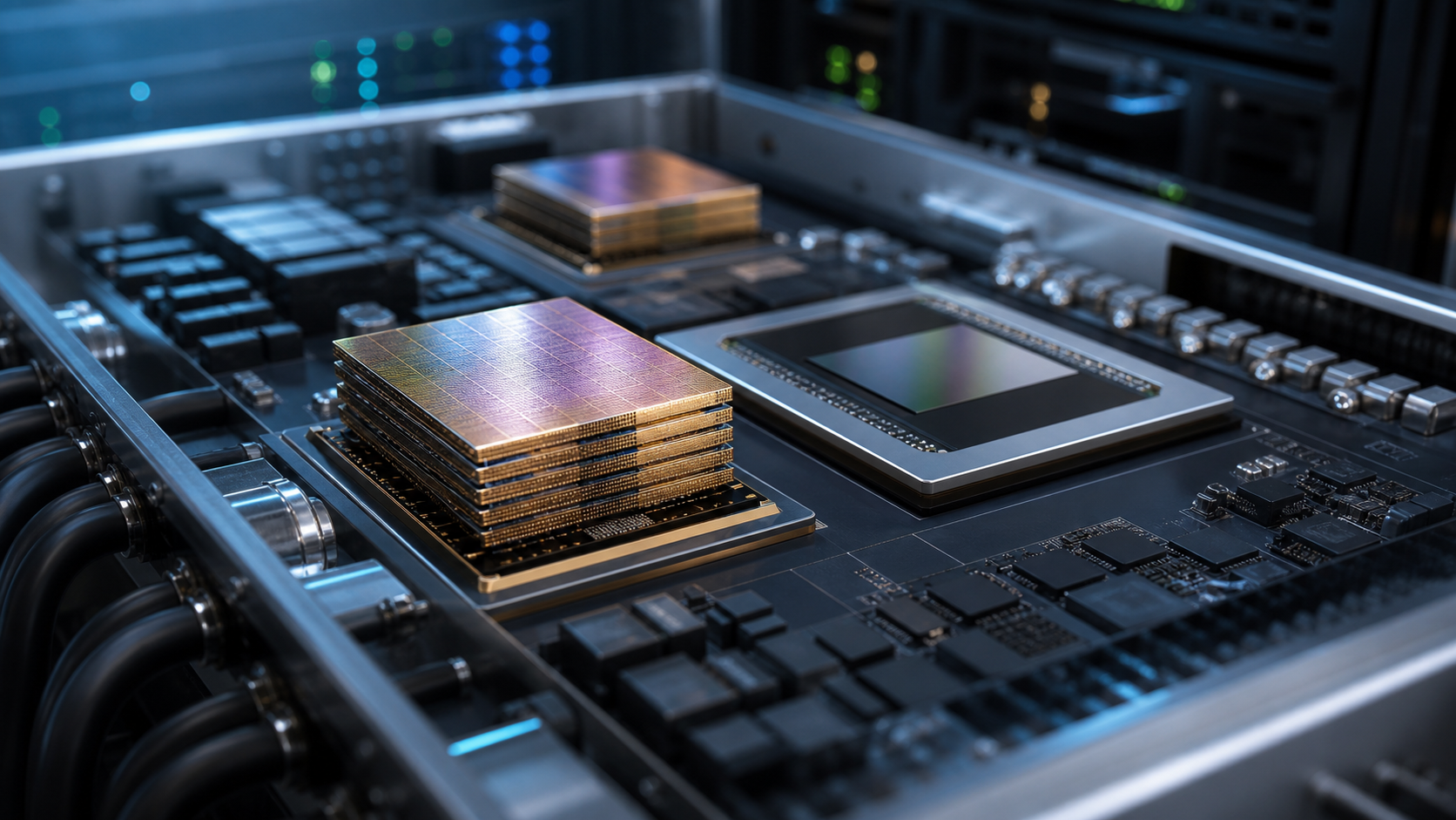
Traditional server DRAM is placed around the CPU socket in the form of DIMMs. GDDR, widely used in graphics cards, also connects a GPU to memory chips outside the GPU package through PCB traces. HBM, by contrast, vertically stacks multiple DRAM dies and places those stacks directly beside a logic chip such as a GPU or ASIC on a silicon interposer. The data travel distance becomes shorter, and a very wide parallel interface can be used, making it possible to obtain enormous bandwidth without pushing single-pin speeds to extreme levels. This approach improves both power efficiency and space efficiency, two factors that are critical in AI data centers.
Competition up to HBM3E was mainly focused on bandwidth of roughly 1TB/s per stack, mass-production stability for 8-high and 12-high products, customer qualification, heat dissipation capability, and yield. Starting with HBM4, the debate becomes broader. Under the JEDEC standard, the interface width doubles to 2,048 bits, the number of independent channels increases, and the base die emerges as a critical component that determines connection quality, power management, and signal management between the logic chip and the memory stack, rather than merely serving as a lower connection layer. In addition, as 12-high and 16-high stacks become major topics, package height, thermal resistance, TSV alignment, micro-bumps or next-generation bonding technologies, interposer area, and the investment burden across the supply chain all increase as well.
This article is an updated version of the previous HBM3E-centered discussion, revised around HBM4 and HBM4E. The core argument is twofold. First, the history of HBM should be understood as a sequence of technological accumulation from HBM1 through HBM3E. Second, HBM4 and HBM4E are not simple component upgrades. They are changes that affect the design methods of next-generation AI server platforms such as NVIDIA Vera Rubin and AMD Helios, the product strategies of memory suppliers, the foundry and packaging ecosystem, and even cloud service providers’ total cost of ownership calculations.
The Basic Structure of HBM: What 2.5D and 3D Memory Mean
HBM stands for High Bandwidth Memory. As the name suggests, its central goal is high bandwidth. But if we emphasize bandwidth alone, it is easy to miss the essence of HBM. HBM is a memory system that combines a 3D structure, in which DRAM dies are stacked vertically, with a 2.5D packaging structure, in which memory stacks are placed next to a logic chip such as a GPU or ASIC. Multiple DRAM dies are connected by TSVs, or Through-Silicon Vias. A TSV is an electrical pathway that vertically penetrates a silicon die and allows each stacked DRAM die to communicate with the base die below.
An HBM stack is usually described as having a base die at the bottom, with DRAM dies stacked above it. The base die is becoming more important with each HBM generation. In earlier generations, its role as the lower interface of the DRAM stack was emphasized. In HBM4, however, it plays a larger role in improving the connection between the logic chip and the HBM stack, power distribution, signal integrity, channel management, and thermal and power characteristics. Samsung Electronics has mentioned 4nm foundry logic and base die technology in its description of HBM4, while SK hynix has also explained that HBM4 improves connectivity between the HBM stack and logic chip and reduces power consumption by improving base die performance. This shows that HBM is becoming a system component that combines logic and packaging technology, not merely a DRAM product.
The area where HBM is placed beside a GPU or AI ASIC is not an ordinary PCB but a silicon interposer. The interposer is an intermediate substrate that connects the logic chip and multiple HBM stacks with short, dense wiring. Thanks to this structure, HBM can use thousands of input and output lines. Rather than relying on very high pin speeds like GDDR, it secures bandwidth by using a much wider bus in parallel. Rambus’ HBM explainer also identifies this 2.5D and 3D structure, stacked DRAM connected by TSVs, and placement on a silicon interposer beside a GPU or ASIC as the core characteristics of HBM.
This structure creates both advantages and costs. The advantages are overwhelming bandwidth, lower data movement energy, a smaller footprint, and proximity to the logic chip. The costs are advanced packaging difficulty, larger interposer area, TSV and stacking yield issues, heat dissipation, and supply-chain bottlenecks. As the number of accelerators in each AI server increases and the number of HBM stacks per accelerator rises, HBM is no longer just a memory cost. It is now a key variable in the total cost, delivery schedule, and power design of an entire AI server.
The History of HBM: From HBM1 to HBM3E
HBM began as an attempt to overcome the bandwidth limitations of the existing GDDR approach in GPUs and high-performance computing. AMD and SK hynix played important roles in early HBM development, and AMD’s Fiji GPU is often mentioned as one of the first commercial examples. HBM1 was standardized and productized around 2013 to 2014, and as it was applied to high-performance graphics products around 2015, it proved that a different approach to memory placement was possible.
The significance of HBM1 lies more in its structural shift than in its numerical specifications. Instead of placing multiple memory chips around a GPU and sending high-speed signals over relatively long distances, HBM validated the concept of stacking memory and placing it next to the logic chip with a very wide interface in a real product. At the time, its use was limited because of capacity, cost, and packaging difficulty. However, as AI and HPC demand grew, the advantages of this structure became much more prominent.
HBM2 followed HBM1 and improved speed, density, and applicability. It created a foundation for broader use not only in high-performance graphics, but also in AI training, HPC simulation, networking equipment, and specialized accelerators. HBM2 was an intermediate stage in the transition of HBM from an experimental premium graphics memory to a practical option for data center accelerators. As AI model sizes increased and data-parallel and model-parallel training spread, the idea that memory bandwidth determines accelerator utilization also became widely accepted.
HBM2E can be understood as an extension of HBM2. As explained in the earlier article, HBM2E provided higher capacity and speed than HBM2, and bandwidth exceeding 460GB/s per stack and capacity of up to roughly 16GB per stack were discussed. This generation served as a bridge for handling larger datasets and models in AI and HPC applications. It also laid the foundation for the HBM market to reorganize into a serious competitive field among SK hynix, Samsung Electronics, and Micron.
HBM3 appeared with the goal of delivering higher bandwidth and capacity than HBM2E. As mentioned in the earlier article, early HBM3 discussions referred to bandwidth of up to roughly 819GB/s per stack, and it became a generation designed to meet the demands of data-intensive applications. As training for large language models exploded, HBM3 moved to the center of the AI accelerator supply chain. Its importance became clear in data center GPUs such as NVIDIA H100, and the later transition to HBM3E accelerated performance competition in AI servers even further.
HBM3E is an extension of HBM3. Rambus describes HBM3E as operating at 9.6Gb/s with a 1,024-bit interface and approximately 1,229GB/s per device. In the HBM3E race, SK hynix, Samsung Electronics, and Micron emphasized speed, bandwidth, 8-high and 12-high stacking, customer qualification, and power efficiency. Samsung and Micron discussed bandwidth at roughly the 1.2TB/s level, and SK hynix also built a strong position in the AI server market with HBM3E and 12-high products. HBM3E became an important component in Blackwell-generation platforms such as NVIDIA GB200.
Competition up to HBM3E was not simply the popularization of high bandwidth memory. It was the transformation of HBM into an essential component of advanced AI servers. GPU manufacturers and cloud service providers demanded greater HBM capacity and bandwidth, while memory suppliers had to invest heavily in TSV processes, stacking technology, packaging materials, heat dissipation, and yield improvement. This trend expands further with HBM4. HBM4 is not merely a faster version of HBM3E. It is a generation that changes interface width, channel structure, base dies, stacking height, and platform design at the same time.
| Generation | Introduction and commercialization trend | Interface and bandwidth characteristics | Capacity and stacking characteristics | Main significance |
|---|---|---|---|---|
| HBM1 | Introduced around 2013 to 2014; AMD Fiji GPU is a representative early commercial example | Used a wide parallel interface and 2.5D packaging to ease the bandwidth limits of conventional GDDR | Stage for validating the early stacked HBM structure | Proved in commercial products a new memory model that places stacked DRAM beside a GPU |
| HBM2 | Expanded after HBM1 into AI, HPC, and professional graphics | Improved speed and density compared with HBM1 | Expanded capacity usable in high-performance accelerators | Created the basis for HBM to move beyond premium graphics and become data center accelerator memory |
| HBM2E | Announced and spread around 2018 to 2019 | Based on the earlier article, bandwidth exceeding 460GB/s per stack was discussed | Based on the earlier article, described as up to roughly 16GB per stack | Transitional generation that supported larger models and datasets in AI and HPC |
| HBM3 | Details and productization expanded after 2020 to 2021 | Based on the earlier article, bandwidth of up to roughly 819GB/s per stack was discussed | Responded to large-scale AI training demand through high-capacity stacks | Rose as the core memory for data center AI GPUs |
| HBM3E | Expanded as core AI server memory in 2024 to 2025 | According to Rambus, 9.6Gb/s, 1,024 bits, and approximately 1,229GB/s per device | 12-high products and 36GB-class products were mentioned in relation to NVIDIA GB200 and similar systems | Generation that met the bandwidth and capacity requirements of Blackwell-generation AI servers |
| HBM4 | Samples, mass production, and platform adoption announcements in 2025 to 2026 | According to JEDEC, 2,048 bits, up to 8Gb/s, and up to 2TB/s per stack. Some supplier products present higher pin speeds and bandwidth | According to JEDEC, supports 4-high, 8-high, 12-high, and 16-high stacks and 24Gb and 32Gb die densities, with up to 64GB cube density using 32Gb 16-high | Transition to core memory for NVIDIA Vera Rubin and AMD Helios and MI400-class platforms |
| HBM4E | Follow-on generation for which 2026 sampling and expansion around 2027 are discussed | Based on Rambus and Samsung descriptions, 16Gb/s with a 2,048-bit interface suggests roughly 4.0 to 4.096TB/s-class potential | Discussion expands around custom base dies and customer-specific HBM | Potential evolution after standard HBM4 into memory tailored for customer-specific AI ASICs and next-generation accelerator platforms |
A Closer Look at HBM4: What the 2,048-Bit Interface Means
The most symbolic change in HBM4 is the 2,048-bit interface. Compared with the 1,024-bit interface commonly associated with HBM3E-class products, the width is doubled. In simplified terms, memory bandwidth is calculated by multiplying the transfer speed per pin by the interface width. Therefore, even at the same pin speed, doubling the interface can greatly increase theoretical bandwidth. JEDEC’s HBM4 standard announcement presents a 2,048-bit interface, transfer speeds up to 8Gb/s, and bandwidth of up to 2TB/s per stack. Rambus also explains that HBM4 reaches 2.048TB/s per stack at 2,048 bits and 8Gb/s.
This change does not merely mean that the numbers have grown larger. AI accelerator designers can use more memory channels and wider data paths to supply data to compute cores. In large-scale model training, matrix computation itself is important, but continuously supplying weights and activations is also essential. In inference, especially when handling long contexts and many simultaneous user requests, KV cache and intermediate data movement can become bottlenecks. HBM4 is designed in a direction that reduces these data-movement bottlenecks.
However, when the interface width doubles, packaging difficulty also increases. More input and output lines, more complex interposer wiring, stricter signal integrity management, denser micro-bump or bonding structures, and larger power delivery networks are required. HBM must create thousands of stable connections in a narrow space, so with each generation, the roles of foundries, OSAT companies, packaging materials suppliers, and test equipment companies grow along with those of memory suppliers.
The 2,048-bit interface of HBM4 also directly affects GPU or ASIC package design. The number of HBM stacks placed on the interposer, the distance between the logic die and HBM, the number of wiring layers, package area, and cooling structure can all change. If the interposer becomes larger, cost and yield burdens increase, and if the package becomes larger, the server board and cooling solution are also affected. Therefore, an AI accelerator adopting HBM4 is not a product in which only the memory chip has changed; the entire module and server design change with it.
HBM4 Channel Structure: 32 Independent Channels and Pseudo-Channels
Another important change in JEDEC’s HBM4 standard announcement is the number of channels. HBM4 is described as increasing from 16 independent channels in HBM3 to 32 independent channels, with each channel having two pseudo-channels. Simply put, HBM4 manages the wider 2,048-bit interface through a more segmented channel structure to improve parallelism. Here, a pseudo-channel can be understood as a concept that divides a physical channel into smaller access units so that memory requests can be handled more efficiently.
In AI workloads, memory access patterns are not uniform. During training, large tensors may move sequentially, but in inference, request lengths and batch sizes vary. In MoE models, different experts may be activated, and in long-context scenarios, cache access grows. If the channel and pseudo-channel structure is more segmented, the memory controller can schedule a variety of accesses more flexibly. Of course, actual performance depends not only on HBM itself, but also on the GPU or ASIC memory controller, cache hierarchy, software optimization, and model architecture.
One point to watch here is that standard numbers, product numbers, and real server performance are different. The JEDEC standard defines interoperability and a basic range. However, companies such as Samsung Electronics, SK hynix, and Micron can satisfy the standard while also offering higher pin speeds, better power efficiency, and specific capacity configurations to meet customer requirements. For example, Samsung Electronics has mentioned consistent operation at 11.7Gb/s for HBM4, potential operation up to 13Gb/s, and up to 3.3TB/s bandwidth per stack. These figures should be read separately from JEDEC’s standard 8Gb/s number.
The Base Die: Lower-Level Logic That Becomes More Important in HBM4
In HBM4, the base die is a very important keyword. An HBM stack is not simply a structure in which DRAM dies are piled upward. At the bottom of the stack is a base die, and that base die connects the DRAM dies above with the logic chip or interposer below. As HBM generations advance, interface width, channel count, power management, and signal quality requirements all increase, raising the design difficulty of the base die.
Samsung Electronics describes HBM4 as being based on 1c DRAM and 4nm foundry logic and base die technology. This shows the direction in which a memory company is trying to combine foundry logic processes with HBM to make the lower part of the stack more sophisticated. SK hynix also introduced HBM4 at Computex Taipei 2025 and explained that improved base die performance increases connectivity between the HBM stack and the logic chip while reducing power. Micron has also mentioned HBM4 for NVIDIA Vera Rubin, 36GB 12H products, bandwidth exceeding 2.8TB/s, and approximately 20% energy efficiency improvement. Each supplier uses different wording, but the shared point is that HBM4 is a system-level competition involving base dies and packaging, not merely a race over DRAM cells.
As the base die becomes more important, discussion of custom HBM naturally grows. Customer-specific AI ASICs or GPUs may have different requirements for memory interfaces, power budgets, package structures, signal specifications, and RAS functions. This is why HBM4E and custom HBM attract attention after standard HBM4 spreads first. TrendForce expects HBM4E and custom HBM to become mainstream after standard HBM4 and has mentioned discussions around customer-specific base dies for customers such as Google, Meta, and NVIDIA. However, this is an industry forecast and should be distinguished from official shipments of specific server models.
TSVs, Interposers, and 12-High and 16-High Stacks
HBM’s vertical stacking is difficult to achieve without TSVs. TSVs are pathways that penetrate DRAM dies vertically so that electrical signals can move up and down. Accurately aligning and stacking multiple dies, connecting each die, and enabling communication with the base die at the bottom require extremely high process precision. As the number of stacked layers increases, TSV alignment, die thinning, thermal expansion mismatch, warpage, bonding quality, and test difficulty all increase together.
The HBM4 standard is described as supporting 4-high, 8-high, 12-high, and 16-high stacks. 12-high stacks are already mentioned as important configurations in HBM3E and early HBM4 products, while 16-high is the direction needed for higher capacity. JEDEC’s announcement mentions 24Gb or 32Gb die densities and up to 64GB cube density in a 16-high 32Gb configuration. Samsung Electronics has described HBM4 12-high products as 24GB to 36GB and 16-high products as up to 48GB. As this shows, the maximum configuration possible under the standard and the commercial product configurations actually announced by each supplier can differ, so they should be distinguished.
When the number of stacked layers increases, capacity rises, but thermal challenges also grow. Heat generated in upper dies has limited paths to move downward or escape externally, and in high-performance AI servers, the GPU itself also produces a great deal of heat. Therefore, in HBM4, not only power efficiency but also thermal resistance and heat dissipation performance become important marketing points. Samsung Electronics has mentioned a 40% improvement in power efficiency, 10% improvement in thermal resistance, and 30% improvement in heat dissipation for HBM4 compared with HBM3E. Samsung GTC 2026 materials explain that hybrid copper bonding can support stacking of 16 layers or more while reducing thermal resistance by more than 20% compared with conventional thermocompression bonding. This suggests that bonding technology may become a differentiating factor in HBM4E and later generations.
The interposer is also a bottleneck. If more HBM stacks are attached and each stack uses a 2,048-bit interface, the number of wires and package complexity increase. Large AI accelerators have huge logic dies themselves and sometimes include multiple logic chiplets. Connecting multiple HBM stacks to such devices makes silicon interposer area, yield, and manufacturing cost important constraints. In other words, competitiveness in the HBM4 era includes not only DRAM wafer processes, but also advanced packaging capacity and stable interposer supply.
Power and Heat: Why HBM4 Emphasizes Efficiency as Much as Performance
Power is one of the biggest constraints in AI data centers. As GPU performance rises, power density per rack increases sharply, and air cooling alone is often insufficient, accelerating the adoption of liquid cooling. Memory accounts for a non-negligible share of total power. Because HBM has a shorter data travel distance and uses a wide bus compared with GDDR, it has an advantage in power efficiency. However, as bandwidth and capacity per stack increase, absolute power and thermal management difficulty still grow.
JEDEC’s HBM4 standard announcement mentions VDDQ options of 0.7V, 0.75V, 0.8V, and 0.9V, along with VDDC options of 1.0V and 1.05V. Various voltage options broaden the range from which customers and platform designers can choose according to performance, power, signal margin, and product configuration. Rambus also mentions more channels, voltage flexibility, DRFM, and RAS improvements in HBM4 and HBM4E. In data center memory, not only raw speed but also error management, reliability, and serviceability are important, so RAS functions are becoming increasingly important.
Samsung Electronics emphasizes low-power TSV I/O, PDN optimization, power efficiency, thermal resistance, and heat dissipation improvements in HBM4. SK hynix has mentioned improved base die performance and reduced power in HBM4. Micron has presented approximately 20% energy efficiency improvement in HBM4. Because each company uses different criteria and comparison targets, direct comparison of the figures requires caution, but the direction is clear. HBM4 competition is both a contest over TB/s bandwidth and a contest over bandwidth per watt.
Power and heat also affect the economics for server users. To reduce cost per token in AI inference, a system must process more tokens with the same power or achieve the same performance with fewer GPUs and less power. NVIDIA explains that the Rubin platform targets lower token cost and fewer GPU requirements for agentic AI, reasoning, long context, and MoE training and inference. Achieving this goal requires not only compute performance and networking, but also the bandwidth, capacity, and power efficiency of HBM4.
How to Read Supplier Announcements About HBM4
Numbers related to HBM4 vary depending on who announces them and what criteria they use. JEDEC’s standard announcement presents a standard range of up to 8Gb/s, 2,048 bits, and up to 2TB/s per stack. Rambus explains 2.048TB/s using the same structure. Samsung Electronics, by contrast, has mentioned consistent operation at 11.7Gb/s, potential operation up to 13Gb/s, up to 3.3TB/s per stack, and 2.7 times the bandwidth of HBM3E in commercial product announcements. This should be interpreted as a product implementation above the standard.
SK hynix presented 12-layer HBM4 and 12-layer HBM3E at Computex Taipei 2025 and described HBM4 as an industry-leading 2TB/s-class HBM. It also stated that it shipped 12-layer HBM4 samples to major customers in March 2025, planned mass production in the second half of 2025, and had a 16-layer HBM4 roadmap for 2026. Samsung Electronics announced HBM4 mass production and commercial product shipments and mentioned 12-high configurations of 24GB to 36GB and 16-high configurations up to 48GB. Micron mentioned HBM4 for NVIDIA Vera Rubin, 36GB 12H, bandwidth exceeding 2.8TB/s, and about 20% energy efficiency improvement in investor communications.
All of these announcements are important, but it is difficult to place them in one table and rank them simply. Pin speed, bandwidth per stack, capacity, power efficiency, thermal characteristics, customer qualification, actual mass-production yield, delivery schedule, and price are different axes. AI server customers do not seek only the fastest HBM. They evaluate compatibility with a specific GPU or ASIC package, long-term supply availability, power and thermal conditions, yield and defect rates, and system-level reliability together. Therefore, the winner in the HBM4 market is likely to be the supplier that can deliver products suited to customer platforms at scale and on time, rather than the supplier with the number-one specification in a single category.
HBM4E and Custom HBM: The Battlefield After the Standard
HBM4E can be understood as an extension of HBM4. Just as HBM3E raised the speed and capacity of HBM3, HBM4E is likely to pursue higher pin speeds, higher bandwidth, and customer-specific functions based on HBM4’s 2,048-bit structure. Rambus describes HBM4E as approximately 4.096TB/s per device based on 16Gb/s and a 2,048-bit interface. Samsung GTC 2026 materials also state that HBM4E will provide 16Gb/s per pin and 4.0TB/s bandwidth. Samsung’s HBM4 shipment announcement mentions that HBM4E sampling is expected in the second half of 2026 and that custom HBM samples are mentioned for 2027.
The especially important word in HBM4E is custom. The AI accelerator market is not driven only by general-purpose GPUs. Large cloud service providers develop their own AI ASICs or try to use accelerators optimized for specific workloads. Google, Meta, Amazon, Microsoft, OpenAI, and others all have incentives to optimize chips, networks, servers, and software stacks together in order to reduce AI infrastructure costs. In this environment, standard HBM alone may not be enough. Customer-specific base dies, power and signal characteristics, package connection methods, RAS functions, and thermal design may all become differentiators.
In a January 2026 report, TrendForce forecast that HBM4E and custom HBM would become mainstream after standard HBM4. It also mentioned industry observations that Samsung’s custom HBM4E design was targeting around May to June 2026, expectations that SK hynix and Micron were moving in a similar direction, an HBM4E launch in 2027, and an HBM5 outlook for 2029. However, these are industry reports and forecasts. Actual product names, customer adoption, and server shipment timing can only be confirmed through official announcements from the companies involved.
HBM4E and custom HBM also change the business model of memory suppliers. Commodity DRAM is largely a standard product sold to many customers, but custom HBM requires customer-specific design participation, long-term supply agreements, early joint validation, reservations for advanced packaging capacity, and base die design collaboration. This can improve profitability, but it also increases customer concentration and development risk. If a specific customer’s platform schedule is delayed, the memory supplier’s mass-production plan may also be affected. Conversely, a supplier that receives customer qualification first can secure a high barrier to entry.
Confirmed HBM4 Server Platforms and Likely HBM4E Platform Families
When discussing where HBM4 will be used, it is necessary to distinguish confirmed facts from estimates. Based on official materials, representative confirmed platforms include the NVIDIA Vera Rubin family and AMD Helios and MI400 family. NVIDIA explains that the Rubin platform includes the Vera CPU, Rubin GPU, NVLink 6, ConnectX-9, BlueField-4, and Spectrum-6, and states that the Rubin GPU uses HBM4. Vera Rubin NVL72 is a rack-scale system combining 72 Rubin GPUs and 36 Vera CPUs, while HGX Rubin NVL8 is described as an 8-GPU server-board-class configuration. DGX SuperPOD expands Rubin systems to a larger scale.
AMD has also officially presented MI400 and Helios. MI350 is described as a generation using 288GB of HBM3E and up to 8TB/s bandwidth, while MI400 is targeted for 2026 and is described as offering up to 432GB of HBM4, 19.6TB/s memory bandwidth, FP4 and FP8 performance, and scale-out bandwidth. AMD’s Helios page describes integration of 72 MI455X GPUs, 31TB of HBM4 per rack, 19.6TB/s bandwidth per GPU, 260TB/s scale-up bandwidth, and 43TB/s scale-out bandwidth. This shows that HBM4 is becoming a core design variable not only for individual accelerator components, but also for rack-level AI systems.
HBM4E platforms must be discussed much more cautiously. Samsung and Rambus materials describe the possibility of 16Gb/s and roughly 4TB/s-class bandwidth for HBM4E, but confirmed official examples of specific server models using HBM4E are limited. Based on industry forecasts, HBM4E is likely to be adopted around 2027 in next-generation GPU refreshes, customer-specific AI ASICs, proprietary accelerators from large CSPs, and inference platforms requiring longer context and larger memory capacity. However, it is still too early to attach specific names and speak conclusively.
| Platform or server family | HBM generation | Confirmation level | Official or publicly disclosed key details | Interpretation and caution |
|---|---|---|---|---|
| NVIDIA Vera Rubin NVL72 | HBM4 | Officially confirmed | Rubin GPU uses HBM4. NVL72 is described as a configuration with 72 Rubin GPUs and 36 Vera CPUs | Rack-scale platform targeting agentic AI, reasoning, long context, and MoE training and inference. Actual memory capacity and configuration must be checked by product announcement |
| NVIDIA HGX Rubin NVL8 | HBM4 | Officially confirmed | Mentioned as an 8-GPU server-board-class Rubin platform. Rubin GPU uses HBM4 | OEM servers may offer various chassis and cooling configurations, but detailed system specifications can differ by manufacturer |
| NVIDIA DGX Rubin and DGX SuperPOD family | HBM4 | Official platform direction confirmed | An ecosystem scaling Rubin systems to DGX and SuperPOD levels has been presented | Ecosystem adopters such as Microsoft, CoreWeave, AWS, Google, Meta, OpenAI, OCI, Dell, HPE, Lenovo, and Supermicro are mentioned, but individual purchase volumes and configurations require separate confirmation |
| AMD MI400 family | HBM4 | Officially confirmed | MI400 in 2026 is described with up to 432GB of HBM4 and 19.6TB/s memory bandwidth | A key transition point in AMD’s data center GPU roadmap from MI350 with HBM3E to HBM4 |
| AMD Helios with MI455X | HBM4 | Officially confirmed | Described as 72 MI455X GPUs, 31TB of HBM4 per rack, 19.6TB/s per GPU, 260TB/s scale-up, and 43TB/s scale-out | In rack-level design, HBM4 capacity and bandwidth connect directly to model size, context length, and support for multi-agent workflows |
| Proprietary AI ASIC servers from large CSPs | HBM4E or custom HBM | Likely, but not confirmed by model | TrendForce mentions customer-specific base dies and custom HBM4E trends for Google, Meta, NVIDIA, and others | This is an industry forecast, not official shipment of a specific server model. It is safer to view it as a platform family around 2027 |
| Next-generation GPU and ASIC refresh platforms | HBM4E | Possible, details unconfirmed | Rambus and Samsung materials describe HBM4E at 16Gb/s and roughly 4TB/s-class bandwidth | If HBM4E matures, it may be used for higher token throughput and memory-intensive workloads, but actual adoption depends on customer qualification and mass-production schedules |
Server Usage Scenarios: Training, Inference, Long Context, and MoE
The area where HBM4 will likely be felt first is training for extremely large models. As the number of model parameters grows and training data increases, communication between accelerators becomes important, but memory bandwidth for reading and writing tensors inside each accelerator is also critical. HBM4’s wider interface and higher bandwidth per stack can help reduce the time GPU cores spend waiting for data. Of course, actual training performance is also determined by compute performance, networking, software parallelization strategy, and the data pipeline.
In inference, HBM capacity becomes especially important. When serving large models, if all weights and cache do not fit in memory, batch size and concurrent throughput are limited. In long-context inference, KV cache grows, and as the number of users increases, memory requirements rise. The capacity expansion of HBM4 and HBM4E, 12-high and 16-high stacks, and higher bandwidth can help reduce cost per token in long-context and high-concurrency inference.
MoE models are also sensitive to HBM. MoE architectures have very large total model parameters, but activate only some experts during inference. In theory, they can reduce computation, but memory capacity and bandwidth are important in order to quickly fetch the required expert parameters and efficiently batch many requests. NVIDIA’s mention of MoE training and inference as target workloads for the Rubin platform is aligned with this trend.
Agentic AI and multi-agent workflows also increase HBM demand. Moving beyond a structure that simply answers a single question briefly, workloads that combine multi-step reasoning, tool calls, retrieval, code execution, and long-term memory access lead to longer processing time per request and more intermediate state data. AMD Helios is described as targeting larger models, longer context windows, and multi-agent workflows for the same reason. In these workloads, stable memory supply and rack-level scalability are more important than simple peak FLOPS.
Implications for Investment and Industry
The transition to HBM4 is a major opportunity for memory suppliers. While commodity DRAM prices are sensitive to the business cycle, HBM can earn relatively high added value through AI server demand, long-term supply contracts, and customer qualification. But there are not only opportunities. HBM production requires TSVs, stacking, advanced packaging, testing, materials, and customer-specific validation. If yield is low or customer qualification is delayed, the cost burden can grow. In addition, if dependence on certain large customers rises, bargaining power issues and schedule risk appear together.
The impact on foundries and packaging companies is also significant. HBM4 increases the importance of base dies, interposers, and advanced packaging. A company like Samsung, which has memory, foundry, and packaging capabilities, can emphasize the advantages of vertical integration. SK hynix and Micron also compete through customer collaboration, packaging technologies, and materials and equipment ecosystems. For AI accelerator companies, HBM supply stability becomes a key risk to product launch schedules.
Cloud service providers do not view HBM4 as merely a performance improvement. They evaluate it together with rack-level power, cooling cost, cost per token, model serving efficiency, and data center construction speed. Even if HBM4 servers are more expensive, they become economically attractive if they can process the same work with fewer racks and less power. Conversely, if software cannot make sufficient use of HBM4 bandwidth, or if network, storage, and CPU bottlenecks remain, efficiency may not reach expectations.
From an investor’s perspective, it is important to distinguish whether HBM4 and HBM4E are structural growth drivers that can improve memory suppliers’ profitability, or highly volatile businesses excessively dependent on a specific AI investment cycle. When AI server demand is strong, HBM can deliver high margins and pre-order effects. But if supply increases sharply or the pace of investment by major customers is adjusted, prices and utilization rates can fluctuate. In addition, HBM4E and custom HBM carry higher development costs and customer-specific risks, so they may widen the gap between successful suppliers and latecomers.
Important Cautions: Why Specifications Alone Are Not Enough
First, standard numbers and supplier-announced numbers must be distinguished. The JEDEC HBM4 standard presents an 8Gb/s and 2TB/s-class range, while Samsung mentions up to 13Gb/s and 3.3TB/s, and Micron mentions bandwidth exceeding 2.8TB/s. This does not mean the numbers contradict each other. It means the criteria and product implementations may differ. The standard is a minimum common language, while supplier products can deliver higher performance depending on customer requirements and process capability.
Second, bandwidth per stack is not the same as server performance. Real performance depends on how many HBM stacks are attached to one accelerator, how much capacity each stack has, how the memory controller is designed, and how efficiently cache and software shape memory access. At rack scale, communication between GPUs, CPUs and NICs, storage, power delivery, and cooling can also become bottlenecks.
Third, 16-high stacks raise capacity but also increase difficulty. Stacking more dies increases capacity, but package height, thermal resistance, bonding quality, and yield challenges can grow. Technologies such as hybrid copper bonding attract attention because they can reduce thermal and bonding issues in stacks of 16 layers or more. However, new bonding technologies also require mass-production stability, equipment investment, and customer validation time.
Fourth, HBM4E and custom HBM still involve considerable uncertainty. The 16Gb/s and 4TB/s-class numbers are very attractive, but which customer’s server will ship at volume and when is a separate matter. TrendForce’s outlook for HBM4E in 2027 and HBM5 in 2029 is useful for understanding the direction of the industry, but it is not the same as an official product announcement. Therefore, investment judgments related to HBM4E should examine supply contracts, customer qualification, actual sampling, and mass-production disclosures together.
Conclusion: HBM4 Moves to the Center of AI Server Design
The history of HBM began as an effort to solve memory bottlenecks in GPUs and HPC, and it has grown into a core infrastructure component for AI data centers. HBM1 showed the possibility of the structure, HBM2 and HBM2E expanded the range of applications, and HBM3 and HBM3E became essential memory for large-scale AI accelerators. Now HBM4 is trying to support the next stage of AI servers by widening the interface to 2,048 bits and combining 32 independent channels, a pseudo-channel structure, improved base dies, 12-high and 16-high stacking, and power and thermal optimization.
NVIDIA Vera Rubin and AMD Helios and MI400-class systems show that HBM4 is entering the center of real next-generation platforms. These platforms are not simply faster GPUs. They are AI systems that combine larger memory, higher memory bandwidth, faster scale-up and scale-out networks, higher rack power, and more advanced cooling designs. In such systems, HBM4 is the core data supply chain that feeds the compute engines.
HBM4E and custom HBM are the next stage. Bandwidth of 16Gb/s and roughly 4TB/s-class levels, customer-specific base dies, next-generation bonding technologies, customized RAS, and power design will further segment AI accelerator competition. However, HBM4E is still an area with limited confirmation of specific server models, so official announcements and industry forecasts must be read separately. What is clear is that HBM is no longer an auxiliary component. It has become a strategic bottleneck and differentiating factor in the AI semiconductor ecosystem.
Related topics
Topics to read together: the AI server investment cycle and HBM demand, the structure of the NVIDIA Rubin platform, AMD Helios and the MI400 roadmap, HBM competition among Samsung Electronics, SK hynix, and Micron, advanced packaging and silicon interposers, custom HBM and customer-specific base dies, liquid cooling and data center power infrastructure.
Sources
1. Previous Finconsult article: History of HBM and the Changes HBM3E Will Bring, Korean post ID 1236.
2. Electronics Weekly, coverage of the JEDEC JESD270-4-based HBM4 standard: 2,048-bit interface, up to 8Gb/s, 32 independent channels, pseudo-channels, voltage options, and 4-high, 8-high, 12-high, and 16-high configurations.
3. Rambus HBM explainer, updated March 2026: HBM’s 2.5D and 3D structure, TSVs, silicon interposer, and HBM3E, HBM4, and HBM4E bandwidth descriptions.
4. SK hynix Newsroom Computex Taipei 2025: 12-layer HBM4 and 12-layer HBM3E, HBM4 sample shipments, second-half 2025 mass-production plan, and 2026 16-layer roadmap.
5. Samsung Semiconductor HBM4 page and HBM4 shipment announcement: 2,048 I/O pins, 1c DRAM, 4nm logic and base die, up to 13Gb/s, up to 3.3TB/s, power efficiency, thermal resistance, heat dissipation improvements, and HBM4E sampling outlook.
6. Samsung GTC 2026: HBM4 for NVIDIA Vera Rubin, HBM4E at 16Gb/s per pin and 4.0TB/s bandwidth, and hybrid copper bonding explanation.
7. Micron official investor snippets: HBM4 for NVIDIA Vera Rubin, 36GB 12H, bandwidth exceeding 2.8TB/s, and approximately 20% energy efficiency improvement.
8. NVIDIA official Rubin platform materials: Vera CPU, Rubin GPU, NVLink 6, ConnectX-9, BlueField-4, Spectrum-6, Vera Rubin NVL72, HGX Rubin NVL8, DGX SuperPOD, and HBM4 usage.
9. AMD official MI400 and Helios materials: MI350 HBM3E, MI400 HBM4, Helios with MI455X, 31TB HBM4 rack, 19.6TB/s per GPU, and scale-up and scale-out bandwidth.
10. TrendForce Jan 2026: outlook for HBM4E and custom HBM becoming mainstream after HBM4, customer-specific base dies, HBM4E in 2027, and HBM5 in 2029.
Language versions:
한국어 원문 |
English version