
Language versions:
English version |
Korean version
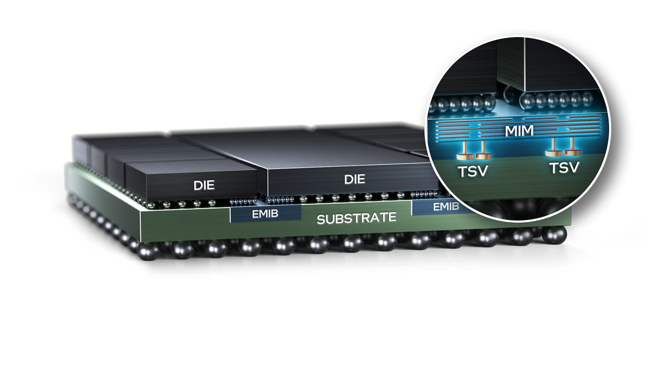
- EMIB-T is Intel’s next evolution of embedded-bridge packaging. It adds through-silicon vias to the bridge so power and signals can move through the bridge, not merely around it.
- TSMC’s reported Kinsus-backed EMIB-like project should be read as a response to CoWoS capacity pressure and customer demand for a lower-cost, more modular path to AI accelerator packaging.
- The technology is cheaper than full-interposer CoWoS in some designs, but it is more than a discount product. It can become a separate class of chiplet fabric for HBM4, UCIe, custom ASICs, and very large AI packages.
Introduction: why EMIB-T suddenly matters
Advanced packaging has moved from a back-end manufacturing detail to one of the most important constraints in artificial intelligence hardware. The reason is simple. AI chips are no longer single chips. They are systems made of logic tiles, HBM stacks, I/O die, retimers, power structures and sometimes optical or networking components. The foundry that can connect those pieces at high bandwidth, acceptable yield and reasonable cost becomes more than a wafer supplier. It becomes the system architect.
That is why EMIB-T matters. Intel’s original EMIB, or Embedded Multi-die Interconnect Bridge, placed small silicon bridges inside an organic substrate only where two dies needed high-density communication. It avoided the need for a full silicon interposer under the entire package. EMIB-T keeps that localized bridge idea but adds TSVs, or through-silicon vias, in the bridge. Intel and Synopsys describe this as a way to improve power delivery, signal routing and high-speed die-to-die communication for the next HBM and UCIe era.
TSMC’s reported work with Kinsus on an EMIB-like technology should be understood in that context. CoWoS remains the premium standard for Nvidia-class AI accelerators, but CoWoS capacity is tight and expensive. Customers such as Google, Broadcom, Meta and other custom ASIC designers want more packaging options. TSMC cannot afford to let Intel become the only credible bridge-based alternative. Kinsus matters because this type of approach shifts more value into high-end substrates and bridge integration, an area where Taiwanese substrate makers can participate.
What EMIB-T is, in plain English
In a conventional 2.5D package, the chiplets usually sit on a large silicon interposer. That interposer gives fine routing lines and can connect logic to HBM with extremely high bandwidth. CoWoS-S is the best-known version of that idea. It works very well, but it uses a large piece of silicon. As AI packages get larger, the interposer becomes expensive, capacity-constrained and mechanically difficult.
EMIB takes a different approach. Instead of placing a full silicon sheet under the whole package, it embeds small silicon bridges in the substrate only where two dies need a dense connection. Intel’s own materials describe this as a cost-effective path for logic-to-logic and logic-to-HBM connections. The bridge creates a high-density shoreline-to-shoreline link, while the rest of the package can remain an advanced organic substrate.
EMIB-T adds the important next step. The bridge now includes TSVs. Those vertical channels let power reach the chips more directly and allow routing through the bridge. This matters for HBM4 and HBM4e because power delivery becomes harder as memory bandwidth, stack height and package size increase. A standard bridge can help with horizontal data movement. A TSV bridge can also become part of the power and signal architecture.
Why the timing changed in 2026
Several forces arrived at the same time. First, the AI accelerator package is getting bigger. Intel Newsroom says advanced packaging in New Mexico can scale packages to eight times the industry reticle standard today and over twelve times by 2028. Tom’s Hardware cites package concepts around 120 mm by 180 mm, more than thirty bridges and more than twelve reticle-sized dies in a single package. Those are no longer normal chips. They are boards inside a package.
Second, HBM4 changes the package power problem. HBM bandwidth is rising, but the energy and current delivery needed to support that bandwidth are rising too. IEEE’s EMIB-T abstract says AI and machine learning demand hyper-large form-factor data center GPUs and CPUs with significant on-package HBM bandwidth. EMIB-T is presented as a cost-effective and high-yielding alternative that can deliver power directly through bridge TSVs from the package bottom to HBM dies.
Third, TSMC’s CoWoS capacity remains structurally tight. TrendForce and TechPowerUp report that TSMC is developing an EMIB-like technology with Kinsus because some customers may consider Intel’s EMIB platform if CoWoS capacity and cost stay difficult. This is not a small side project. It is a defensive and strategic move by the leading foundry.
CoWoS versus bridge-based packaging
The right comparison is not “CoWoS good, EMIB cheap.” That is too simple. CoWoS is an interposer-centric platform. CoWoS-S uses a silicon interposer with TSVs and gives extremely dense routing. CoWoS-L uses localized silicon interconnect elements inside a larger RDL structure, and CoWoS-R relies more heavily on an organic copper/polymer RDL interposer. TSMC already understands that one packaging architecture cannot cover every AI product.
EMIB is localized. It is most attractive when high-bandwidth communication is concentrated between adjacent dies, such as logic-to-HBM or logic-to-logic. If the entire package needs uniform, extremely fine routing everywhere, a full interposer can still be the cleaner answer. If the package only needs fine silicon where the important die edges meet, a bridge can reduce silicon area, cost and supply pressure.
That is why EMIB-T should be viewed as a separate architecture rather than only a cheaper CoWoS substitute. It changes the trade-off among cost, substrate size, HBM power delivery, design freedom and supply chain capacity. In some designs it will be the cheaper answer. In others it may be the only practical answer because a huge full interposer is too expensive or too hard to source.
TSMC and Kinsus: why the substrate partner matters
Kinsus is not a foundry and it does not replace TSMC’s packaging know-how. Its importance is in substrates. Kinsus describes Flip Chip BGA as suitable for very high pin-count chips such as microprocessors, graphics processors, ASICs and FPGAs, where wire bonding is not practical on cost or performance grounds. That is the right industrial neighborhood for EMIB-like packaging.
If TSMC builds an EMIB-like platform with Kinsus, the goal is likely to combine TSMC’s system-integration control with a substrate partner that can help scale the manufacturing base. The reported purpose is not to abandon CoWoS. It is to keep customers inside the TSMC ecosystem when CoWoS is too expensive, too scarce, or not geometrically optimal for a particular chiplet layout.
This matters for AI ASIC customers. Google TPUs, Broadcom-designed accelerators, Meta’s in-house silicon and networking ASICs do not always need the exact same package as Nvidia’s flagship GPUs. A custom ASIC buyer may accept a bridge-based design if it delivers enough HBM bandwidth, lower cost and more capacity certainty. That is a powerful proposition in a market where packaging lead time can decide a product launch.
Samsung Foundry’s move: not EMIB by name, but a broader Cube strategy
Samsung Foundry should also be part of this discussion. Samsung is not marketing a product called EMIB-T, and it is not trying to copy Intel’s naming. Its response is broader: build a menu of 2.5D, 2.3D and 3D packaging options, then connect those options to Samsung’s memory, foundry and test capabilities.
The most relevant part is Samsung’s Advanced Heterogeneous Integration portfolio. Samsung lists 2.5D Cube-S, 2.3D Cube-E, 2.3D Cube-R, 3D Cube-T and 3D Cube-H. Cube-S is the closest to a classic CoWoS-style silicon interposer flow: logic chips and HBM dies sit horizontally on a silicon interposer to create high-bandwidth and low-latency data paths. Samsung says 2.5D packages with a 3.3x silicon interposer, advanced logic and up to eight HBM modules are fully qualified and available for production, with larger versions supporting more than eight HBM modules.
The more interesting Samsung answer to EMIB-like packaging is 2.3D Cube-E. Samsung describes Cube-E as a silicon-embedded structure that combines a fine-patterned silicon bridge, a TSV-less RDL interposer and a large-area interposer enabled by fan-out panel-level packaging. That language matters. It means Samsung is also moving toward localized silicon where it is needed, while trying to keep the cost and mechanical advantages of a larger RDL/fan-out structure.
Cube-R goes one step further toward an organic RDL interposer architecture, while Cube-T and Cube-H address vertical logic stacking through TSV and hybrid Cu-Cu connections. The package menu is therefore not a single CoWoS clone. It is a ladder: full silicon interposer for the most bandwidth-hungry HBM designs, embedded-bridge or RDL approaches for cost and area scaling, and 3D stacking for designs that need shorter vertical interconnects.
Samsung’s second move is turnkey service. Samsung Foundry says it offers an end-to-end process spanning wafer fabrication, bump, package and test, with memory-logic integration and partnerships across OSAT and PCB ecosystems. This is important because Samsung is the only major foundry challenger that also owns leading-edge HBM and DRAM. If Samsung can package a customer logic die with Samsung HBM through a controlled turnkey flow, it has a different pitch from both Intel and TSMC.
The investment implication is balanced. Samsung’s packaging strategy does not yet have the same market pull as TSMC CoWoS or the same bridge identity as Intel EMIB-T. But it gives Samsung Foundry a credible answer for AI customers that want memory, logic and packaging to be optimized together. If HBM4 qualification improves and Cube-E/R mature, Samsung could become a more serious alternative for AI ASICs that need capacity outside the TSMC CoWoS bottleneck.
Who will use EMIB-T and EMIB-like packaging?
The first users are likely to be AI accelerator and custom ASIC companies. The obvious candidates are products that combine large logic dies with HBM stacks and high-speed die-to-die interfaces. Intel’s own roadmap, external foundry customers, Google TPU-style accelerators, Broadcom-linked ASIC programs, Meta AI silicon and high-end networking processors all fit the profile. This does not mean every one of these products will adopt EMIB-T. It means their architectural needs match the problem EMIB-T is designed to solve.
HBM4 is the key trigger. HBM3E packages already stress power and routing. HBM4 increases bandwidth and changes the physical interface. If EMIB-T can reduce voltage droop, improve current delivery and support UCIe-A class links at high speeds, it becomes relevant to the most important AI packages of 2027 and 2028. The reported move by TSMC and Kinsus makes sense because no leading foundry wants Intel to own that conversation alone.
There is also a second group of users: large CPUs, FPGAs, network switches and chiplet-based data-center devices. Intel’s IEEE abstract notes EMIB’s use across FPGAs, server CPUs, GPUs and data-centric HPC. The bridge approach fits products where different chiplets are made on different process nodes and need high-bandwidth links without forcing a single giant die.
The role of EMIB-T in the AI supply chain
EMIB-T can play three roles. The first is capacity relief. If a package does not need a full silicon interposer, bridge-based packaging reduces demand for the most constrained interposer capacity. That helps customers and it also helps TSMC protect front-end wafer demand, because a customer that cannot package an accelerator cannot ship the wafer value either.
The second role is cost control. TechPowerUp reported that the price gap between EMIB-T and CoWoS may be as large as 50 percent depending on the need for an expensive interposer. The exact number will vary by design, yield, substrate size and HBM count, but the direction is clear. Silicon area is not free, and using it only where necessary is economically attractive.
The third role is architecture. This is the part investors should not miss. EMIB-T is not only a procurement workaround. By adding TSVs to the bridge, it can become part of the power-delivery network and the signal-integrity plan. Synopsys highlights TSV-enabled power delivery, dense MIM capacitors, routing for high-speed protocols and design flows that can handle dozens of bridges. That is a system-design function, not a cheap packaging trick.
Is it more than a cheaper CoWoS?
Yes, but with an important qualification. EMIB-T is not superior to CoWoS in every case. A full interposer remains excellent when a design needs extremely dense routing across a broad area. CoWoS also has a large ecosystem, deep production history and direct alignment with Nvidia’s high-volume accelerator roadmap. It will remain the premium option for many frontier GPUs.
EMIB-T becomes more than a cheaper CoWoS when the design problem is local, modular and power-sensitive. If several logic and memory elements need dense edge connections, and if the rest of the substrate does not need silicon-interposer density, bridge packaging is elegant. If power needs to move through the bridge to HBM, EMIB-T becomes even more useful. If the customer also needs supply-chain flexibility, it becomes strategic.
The best way to think about it is this: CoWoS is the big highway. EMIB-T is a network of very dense bridges placed exactly where the traffic is highest. Sometimes a highway is the right answer. Sometimes the bridge network is cheaper, faster to build and easier to expand.
Potential impact on ASE Technology
ASE Technology is not simply a loser if Intel and TSMC push bridge-based packaging. ASE already offers VIPack, 2.5D/3D IC packaging and FOCoS-Bridge. Its FOCoS-Bridge page describes a silicon bridge embedded in a fan-out RDL layer to connect chiplets such as GPUs and HBM. ASE positions it as an alternative to 2.5D silicon interposer packages, using silicon only in specific connection areas and offering similar electrical, signal and power integrity at lower cost without a reticle-size constraint.
That means ASE understands the same direction. The risk is not technological ignorance. The risk is customer control. If TSMC internalizes more bridge-like packaging with Kinsus, some volume that might have gone to OSAT partners can remain inside TSMC’s packaging orbit. If Intel Foundry turns EMIB-T into a full platform for external customers, some advanced packaging decisions may shift from OSAT procurement teams to foundry platform teams.
For ASE, the impact is mixed. It could lose bargaining power in the highest-end AI accelerator programs if foundries bundle wafers and packaging more tightly. At the same time, bridge-based packaging validates ASE’s own FOCoS-Bridge and VIPack direction. Customers that cannot get enough CoWoS capacity may look for qualified OSAT alternatives. ASE can benefit if it positions FOCoS-Bridge as a second source, a design-specific alternative, or a capacity buffer for AI, networking and HPC products.
Investment view
The investment message is that advanced packaging is becoming a competitive moat. For Intel, EMIB-T is one of the few areas where it can compete with TSMC from a position of real technical credibility. Intel does not need to beat TSMC in every front-end node to create value here. If it wins selected packaging programs for AI ASICs, it can rebuild foundry trust from the package upward.
For TSMC, the Kinsus report is defensive but rational. TSMC’s core risk is not that CoWoS becomes obsolete. It is that CoWoS scarcity pushes some customers to try Intel and then stay there. An EMIB-like option keeps the menu broad. It also lets TSMC serve products that do not need the most expensive CoWoS structure.
For Kinsus and other high-end substrate suppliers, the opportunity is larger content per AI package. For ASE, the issue is whether OSAT advanced packaging can remain an independent buying category or whether foundries will absorb more of the architectural control. ASE has credible technology, but the margin pool will depend on who owns customer architecture decisions.
Conclusion
EMIB-T is important because AI hardware is running into package-level limits. Reticle size, HBM power, interposer capacity, substrate warpage, UCIe routing and cost all converge inside the package. A localized silicon bridge with TSVs is a practical answer to that convergence. It is not the only answer, and it will not replace CoWoS everywhere, but it gives AI chip designers another serious path.
TSMC’s reported work with Kinsus confirms the point. The market is not choosing between one premium technology and one cheap substitute. It is building a portfolio of packaging architectures. CoWoS will remain critical for the most demanding full-interposer products. EMIB-T and EMIB-like packaging will matter where local high-density links, HBM power delivery and supply flexibility are more important than blanketing the whole package with silicon.
For investors, the conclusion is straightforward. Watch the package, not only the wafer. The next AI hardware cycle will be shaped as much by bridge placement, substrate capacity and thermal-compression bonding as by transistor density. Intel, TSMC, Kinsus and ASE are all fighting for that layer of value.
Sources
- Intel Foundry, Advanced Packaging Innovations
- Intel Newsroom, Intel’s U.S. Advanced Packaging Enables Next-Generation AI Semiconductors
- Synopsys, Accelerating Next-Generation EMIB-T Packaging
- IEEE Xplore, EMIB-T (TSV) Advanced Packaging Technology
- Tom’s Hardware, Intel details new advanced packaging breakthroughs
- Tom’s Hardware, Intel’s EMIB-T packaging technology set for fab rollout
- EDN, Intel ups the advanced packaging ante with EMIB-T
- TrendForce, TSMC reportedly develops EMIB-like packaging with Kinsus
- TechPowerUp, TSMC Develops EMIB-like Technology to Compete with Intel
- TechPowerUp, Intel’s EMIB-T to Rival TSMC’s CoWoS with 50% Cost Advantage
- SemiWiki, TSMC CoWoS versus Intel EMIB Semiconductor Packaging
- Kinsus, Flip Chip BGA product page
- ASE, VIPack advanced packaging platform
- ASE, FOCoS-Bridge
- ASE, 2.5D and 3D IC Packaging
- Samsung Foundry, Advanced Packaging
- Samsung Foundry, Advanced Heterogeneous Integration
- Samsung Foundry, Package Turnkey Service